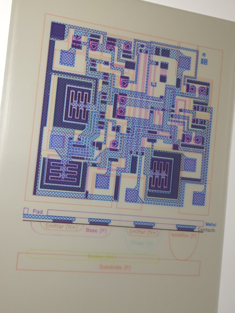
let's separate out a few layers. on the right is the top metal, pad openings, and contact via openings. on the left are the diffusions: isolation, emitter, base, sinker, and buried layer.
this took a surprising amount of work. i traced over an original 555 layout in Inkscape, then used the Axidraw Crosshatch and the Axidraw Hershey Text plugins.
i'm amazed how many bugs i ran into while working on this. Inkscape likes to randomly flip/rotate groups, and the plotter extension sometimes forgets to add pen up commands, so my check plots have diagonal lines all over the place...
I've run into this too - tried to use Inkscape with a Cricut cutter/plotter that uses gcode and ran into all manner of problems with rotation & penup/pendown.

Comments
Actually probably not really. But I live that a huge amount of chip design is from this open source tool & what a great name for it.
I recommend following Martin Owens on YouTube for updates.